Priority encoder 74ls148 pin diagram pin diagram internal function table
Priority encoder 74ls148 pin diagram pin diagram internal function table
Priority encoder 74ls148 pin diagram pin diagram internal function table
In the priority encoder circuit, it is allowed to input more than two encoded signals at the same time. However, when designing a priority encoder, all input signals have been queued in priority order. When there are two or more input signals at the same time, the priority encoder only encodes the input signal with high priority, and the signal with low priority does not work. 74148 is an eight-wire-three-wire priority encoder. As shown in the figure are the usual symbols and pin diagrams of the 8-wire-three-wire encoder 74148.
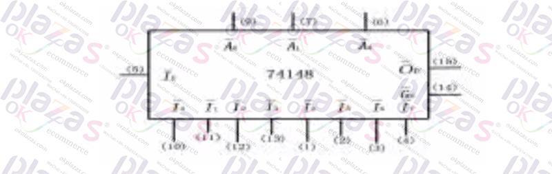
From the 74148 truth table, the output logic equation can be listed as: A1 = (I2I4I5+I3I4I5+I6+7) The logic equation of the IE enable output terminal OE is:
When enabling input IE=1, encoding and output are prohibited (inverse code): A2, A1, A0 are all ones. (As shown in the first row of Table 5.1.2.) OE is the enable output terminal, which is only 0 when encoding is allowed (IE=0) and there is no encoding input in this film. As shown in the second row of Table 5.1.2).
The logic equation of the extended chip priority encoding output terminal GS is:
GS is the output terminal of chip priority encoding. It is 0 when encoding is allowed (IE=0) and there is an encoded input signal (as shown in the third to tenth rows in Table 5.1.2); if encoding is allowed without an encoded input signal It is 1 (as shown in the second row of Table 5.1.2); when encoding is not allowed (IE=1), it is also 1 (as shown in the first row of Table 5.1.2). 74148 priority encoder truth table?

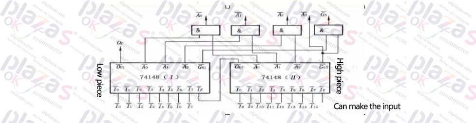
Use two 74148 priority encoders to expand to sixteen-wire-four-wire priority encoder wiring diagram
-
The principle and application field of Autonics panel products (handling)
 June 12, 2021
 -
New product launch SRH1 series single-phase SSR with integrated heat sink
 June 12, 2021
 -
New product launch SRH1 series single-phase SSR with integrated heat sink
 June 12, 2021
 -
Otto protection grade IP69K new product launched Ø18mm cylindrical (SUS316L housing) photoelectric sensor BRQT series
 June 12, 2021
 -
Autonics adds shading motion mode sensor
 June 12, 2021